Vacuum and Surface Science
Online ISSN : 2433-5843
Print ISSN : 2433-5835
Volume 65, Issue 4
Special Feature : Atomically Controllable Synthesis of Novel Materials Using Chemical Vapor Deposition
Displaying 1-10 of 10 articles from this issue
Preface
Special Feature : Atomically Controllable Synthesis of Novel Materials Using Chemical Vapor Deposition
  • Toshitaka KUBO, Masaki TANEMURA
    Article type: Introduction
    2022 Volume 65 Issue 4 Pages 168
    Published: April 10, 2022
    Released on J-STAGE: April 10, 2022
    JOURNAL FREE ACCESS

    Low-dimensional materials, typically exemplified by graphene and beyond-graphene nanomaterials, are one of the hottest topics in nanoscience and nanotechnology. For their synthesis, chemical vapor deposition (CVD) is the powerful method, and the door to the world of atomically controllable synthesis is going to be opened. In this issue, the fundamentals and the state-of-the-art technology in CVD are overviewed.

    Download PDF (233K)
  • Taiki INOUE, Shigeo MARUYAMA
    Article type: Overview
    2022 Volume 65 Issue 4 Pages 169-176
    Published: April 10, 2022
    Released on J-STAGE: April 10, 2022
    JOURNAL FREE ACCESS

    Atomic layer materials including graphene, hexagonal boron nitride, and transition metal dichalcogenides have attracted great attentions due to their unique physical properties. A chemical vapor deposition (CVD) method of atomic layer materials has substantially progressed in the past decades toward realizing the synthesis of large-scale, high-quality, and structure-controlled crystals. In this paper, we briefly summarize the basics of CVD synthesis of atomic layer materials.

    Download PDF (1781K)
  • Hiroki AGO, Takanobu TAIRA
    Article type: Current Topics
    2022 Volume 65 Issue 4 Pages 177-183
    Published: April 10, 2022
    Released on J-STAGE: April 10, 2022
    JOURNAL FREE ACCESS

    We introduce our chemical vapor deposition (CVD) growth of high-quality monolayer and bilayer graphene on epitaxial metal catalysts. An epitaxial Cu(111) film prepared on sapphire substrate allows the synthesis of monolayer graphene whose orientation is registered by the underlying Cu(111) lattice. Pure AB-stacked bilayer graphene was synthesized by long-time CVD, and the bilayer device showed high on-off ratio indicating the band gap opening. Moreover, interlayer 2D nanospace of the bilayer graphene was used to intercalate metal chloride molecules, and the significant reduction of sheet resistance as well as the unique 2D super-structures of metal chloride molecules is observed. We also visualized the graphene CVD process based on radiation-mode optical microscopy (Rad-OM), obtaining important insight into the graphene growth mechanism.

    Editor's pick

    Download PDF (7440K)
  • Katsuhisa MURAKAMI
    Article type: Current Topics
    2022 Volume 65 Issue 4 Pages 184-189
    Published: April 10, 2022
    Released on J-STAGE: April 10, 2022
    JOURNAL FREE ACCESS

    Our recent progress of direct synthesis of graphene on an insulating substrate and its application for a planar type electron emission device using graphene gate electrode are overviewed. A single layer graphene with a grain size up to 200 nm was directly synthesized on an insulating substrate by chemical vapor deposition (CVD) using Ga vapor as a remote catalyst. To avoid a contamination from metal vapor catalysts and high temperature process, catalyst free synthesis of graphene on an insulating substrate by inductively coupled plasma CVD (ICP-CVD) was also developed. A single layer graphene was realized at a low growth temperature of 773 K by two step growth of graphene nucleus and their edges using ICP-CVD. For the device application of the polycrystalline graphene directly deposited on the insulating substrate, the planar type electron emission device using a graphene/oxide/semiconductor structure was developed. The electron emission efficiency of more than 30% and emission current density of more than 100 mA/cm2 were achieved using graphene gate electrode.

    Download PDF (7383K)
  • Yoshitaka TANIYASU, Shengnan WANG
    Article type: Current Topics
    2022 Volume 65 Issue 4 Pages 190-195
    Published: April 10, 2022
    Released on J-STAGE: April 10, 2022
    JOURNAL FREE ACCESS

    Hexagonal boron nitride (h-BN) is an indispensable material for two-dimensional van der Waals (vdW) materials-based devices. Scalable fabrication methods for high-quality h-BN are essential for the industrial applications. In addition, control of the interlayer angles of stacked 2D vdW materials is crucial for tailoring their electrical properties. In this article, we introduce chemical vapor deposition (CVD) growth of single-orientation h-BN. Then we propose an epitaxial intercalation method for vertically stacked h-BN/graphene bilayers with a high uniformity and a controlled interlayer angle.

    Download PDF (4065K)
  • Yasumitsu MIYATA
    Article type: Current Topics
    2022 Volume 65 Issue 4 Pages 196-201
    Published: April 10, 2022
    Released on J-STAGE: April 10, 2022
    JOURNAL FREE ACCESS

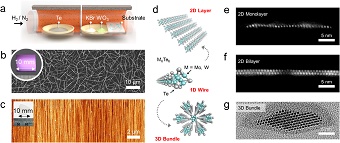
    Recently, atomically-thin layered and wired transition metal chalcogenides (TMCs) have attracted much attention because of their unique physical properties and potential applications. To understand and use these materials, it is still essential to develop large-scale growth processes of such TMC nanostructures with various geometries. In this article, the author introduces the recent progress of the chemical vapor deposition (CVD) growth of layered and wired TMCs. For 2D layered TMCs, metal-organic CVD and direct growth at metal/oxide interface are presented. CVD also provides a powerful way for wafer-scale growth of 1D TMC atomic wires with either aligned, atomically thin 2D sheets or random networks of 3D bundles, both composed of individual wires.

    Download PDF (7206K)
Report
Conference Report
News & Trends
feedback
Top