All issues

Successor
Volume 33, Issue 8
Displaying 1-11 of 11 articles from this issue
- |<
- <
- 1
- >
- >|
Preface
-
Ken NAKAJIMA2012Volume 33Issue 8 Pages 425
Published: August 10, 2012
Released on J-STAGE: August 23, 2012
JOURNAL FREE ACCESSDownload PDF (179K)
Transaction of the 31st Conference on Surface Science [ II ]
-
Yui HARAGUCHI, Takahiro WADA, Yusuke OMINAMI, Nobuaki MATSUDAIRA, Hiro ...Article type: Original
2012Volume 33Issue 8 Pages 426-430
Published: August 10, 2012
Released on J-STAGE: August 23, 2012
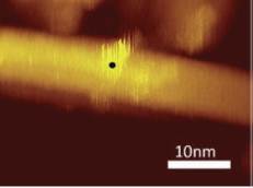
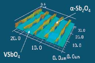 JOURNAL FREE ACCESSWell-defined inhomogeneous α-Sb2O4/VSbO4 catalysts were prepared using an electron lithography method to investigate the effects of µm order structures on an atomic scale catalytic reaction. X-ray photoelectron spectroscopy (XPS) and laser microscopy revealed that µm order structures were successfully developed on a Si substrate where an α-Sb2O4 micro line with a controlled width was deposited on VSbO4. We carried out a propene partial oxidation reaction on this surface and found that the acrolein formation rate was significantly influenced by the width and interval of the α-Sb2O4 µm line. The results of this study indicate the possibility of controlling the surface reaction by the inhomogeneity of the surface structure in the µm order.View full abstractDownload PDF (1488K)
 -
Kenichi TSUTSUMI, Akihiro TANAKA, Masahide SHIMA, Toyohiko TAZAWAArticle type: Original
2012Volume 33Issue 8 Pages 431-436
Published: August 10, 2012
Released on J-STAGE: August 23, 2012
 JOURNAL FREE ACCESSThe chemical state analysis of AES is, at present, performed only for some limited elements. This is because the peak broadness and the shape complexity of Auger spectra make it very difficult to identify the superimposed spectrum as each individual specific chemical state. In this report an advanced chemical state analysis of AES is proposed. This analysis is based on a file of standard spectra of elements with well-defined chemical states, the spectra of which are acquired with high energy resolution of AES. As an example, this method was applied to the depth profile of an tin oxide layer formed on a pure tin plate. The spectra of Sn MNN and O KLL were measured with an energy resolution of 0.1%. Every observed spectra of Sn MNN was separated to three oxidation sates: Sn4+, Sn2+ and Sn0, using the filed standard spectra of SnO2, SnO and Sn. Likewise, O KLL spectra was separated to two bonding state: O2- bonding to Sn2+ and O2- bonding to Sn4+. Moreover, we proposed new quantity method to estimate an atomic concentration depending on the chemical bonding state by comparison with the absolute intensity of the standard spectrum.View full abstractDownload PDF (1120K)
 -
Akihito TAKAHASHI, Daisuke ISHII, Hiroshi YABU, Masatsugu SHIMOMURAArticle type: Current Topic
2012Volume 33Issue 8 Pages 437-442
Published: August 10, 2012
Released on J-STAGE: August 23, 2012
 JOURNAL FREE ACCESSWe fabricated hydrophilic polymer-dome and hydrophobic polymer-pillar hybrid surfaces by using self-organized honeycomb patterned porous films (honeycomb films) consisting of double layer structures. The dome structures were composed of cross-linking polymer between a poly (vinyl alcohol) partially introduced reactive groups (rPVA) and adipic dihydrazide (ADH) as a cross-linker for the reactive groups in the rPVA. Pillar structures were obtained by peeling off the top layer of the honeycomb film. Dome and pillar hybrid surfaces fabricated in this report showed not only superhydrophobicity but also water droplet adhesive property. Ratios of the hydrophilic rPVA-dome in the pillar structures (dome density) were easily adjusted by preparation condition such as a solution temperature. The hybrid surface having 13% dome density was high-adhesive superhydrophobic surface and could keep 9 µL of water droplet when the surface turned upside down.View full abstractDownload PDF (981K)
 -
Takaki SAKAMOTO, Takaaki TOMINAGA, Takahiro NISHIO, Toyoaki EGUCHI, Ya ...Article type: Current Topic
2012Volume 33Issue 8 Pages 443-448
Published: August 10, 2012
Released on J-STAGE: August 23, 2012
 JOURNAL FREE ACCESSUsing low-temperature scanning tunneling microscopy, we have studied superconductivity of nano-size Pb island structures formed on Si(111) substrates. By measuring tunneling conductance at the zero bias voltage, which corresponds to that of the bottom of the superconducting gap, we successfully visualized vortices formed in the superconductors and studied their spatial distributions. Clustering of vortices and a giant vortex structure were observed on islands having void structures.View full abstractDownload PDF (1324K)
 -
Shuichi OGAWA, Takatoshi YAMADA, Shinji ISHIDZUKA, Daiki WATANABE, Aki ...Article type: Current Topic
2012Volume 33Issue 8 Pages 449-454
Published: August 10, 2012
Released on J-STAGE: August 23, 2012
 JOURNAL FREE ACCESSGraphene-on-insulator structures are required for fabrication of the graphene transistor. Diamond has been attracted as the substrate for graphene growth because it has a larger band gap and break down voltage compared with SiC. The detail of graphitization on a diamond surface has not yet been clarified because the nondestructive evaluation for graphene on diamond (GOD) structure was hard. In this study, we have developed the evaluation method of GOD based on the photoemission spectroscopy using synchrotron radiation focusing the shift of photoelectron spectra due to band bending. We can clearly determine the graphitization temperature on the diamond C(111) surface as approximately 1120 K, which is lower than that on an SiC substrate. It is also confirmed from C 1s photoelectron spectra, there is the buffer layer at the interface between the grapheme layer and the diamond substrate.View full abstractDownload PDF (947K)
Current Topics
-
MERA Yutaka, Koji MAEDAArticle type: Current Topic
2012Volume 33Issue 8 Pages 455-460
Published: August 10, 2012
Released on J-STAGE: August 23, 2012
 JOURNAL FREE ACCESSProbing metallic single walled carbon nanotubes (SWNTs) with a tip of scanning tunneling microscope (STM) was found to induce defects in the tubes. Scanning tunneling spectroscopic measurements of local density of states revealed that the defects imaged by STM are characterized by a localized HOMO-LUMO gap of 0.8 eV, which well accounts for the reported metal-semiconductor conversion in SWNT-based field-effect transistor that is induced by low-energy electron irradiation These phenomena, presumably induced by electronic excitations, should be crucial in fabrication processes of SWNT-based electronic devices.View full abstractDownload PDF (818K)
 -
Takaharu OKAJIMA, Yusuke MIZUTANIArticle type: Current Topic
2012Volume 33Issue 8 Pages 461-466
Published: August 10, 2012
Released on J-STAGE: August 23, 2012
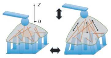 JOURNAL FREE ACCESSThe mechanical properties of live cells are associated with various cell functions, and thus it is crucial to determine the cell elastic modulus, which is one of the fundamental quantities of matter and changes with time and frequency. Atomic force microscopy (AFM) allows us to directly measure the relaxation modulus of single cells in stress and creep relaxation measurements as well as the cell complex modulus in the force modulation. Recent progress in AFM combined with microfabricated substrates revealed the cell-cell variability of cell mechanics, in which the cell modulus exhibits a log-normal distribution depending on the frequency, according to a power-law rheology model. The AFM with micropost substrates as a force sensor demonstrated the direct measurement of intracellular force propagation through cytoskeletal networks between focal adhesions.View full abstractDownload PDF (1889K)
 -
Shinsuke HARA, Katsumi IROKAWA, Hiroki I. FUJISHIRO, Kazuyuki WATANABE ...Article type: Current Topic
2012Volume 33Issue 8 Pages 467-472
Published: August 10, 2012
Released on J-STAGE: August 23, 2012
 JOURNAL FREE ACCESSThe growth processes and structures of Ga layers formed on a Si(001) surface have been studied by scanning tunneling microscopy (STM) and ab initio calculation. The 4×2-Ga structure and the precursor states of the Ga clusters that compose the Si(001) 8×n-Ga (n = 4∼6) structures are observed in addition to the 2×2-Ga structure at a Ga coverage of 0.55 ML at 300oC. We performed an ab initio calculation of the energetics for several possible models for the 4×2-Ga structure, and clarified that the three-orthogonal-Ga-dimer model is the most stable. Also, we compare the observed STM images with the simulated ones to identify the possible structural models of the 4×2-Ga structure and the precursor state of the Ga clusters.View full abstractDownload PDF (1255K)
Science Café
Research Abroad
-
Soh RYUZAKI2012Volume 33Issue 8 Pages 473-474
Published: August 10, 2012
Released on J-STAGE: August 23, 2012
JOURNAL FREE ACCESSDownload PDF (476K)
News & Trends
-
2012Volume 33Issue 8 Pages 475
Published: August 10, 2012
Released on J-STAGE: August 23, 2012
JOURNAL FREE ACCESSDownload PDF (178K)
- |<
- <
- 1
- >
- >|