巻号一覧

後続誌
33 巻, 10 号
選択された号の論文の10件中1~10を表示しています
- |<
- <
- 1
- >
- >|
巻頭言
-
飯島 澄男2012 年 33 巻 10 号 p. 545
発行日: 2012/10/10
公開日: 2012/10/27
ジャーナル フリーPDF形式でダウンロード (180K)
特集:カーボン系材料の特異な表面科学
-
吹留 博一原稿種別: 研究紹介
2012 年 33 巻 10 号 p. 546-551
発行日: 2012/10/10
公開日: 2012/10/27
 ジャーナル フリーFusion of graphene with the substrates adequate for device applications is effective to solve the Year 2020 problem in electronics. Epitaxy of graphene on Si substrate (GOS) has been developed because the choice of Si as the substrate brings two merits, excellent electronic properties of graphene and accumulated device technologies of Si. It is found that electronic properties of GOS can be tuned by substrate interaction through surface termination as well as surface symmetry whose importance has been pointed by the author. Furthermore, epitaxy of GOS on microfabricated substrates has been developed because the GOS technology is to be conformed with future device integrations. GOS on microfabricated substrates with various facets will enable to produce nanoscale multifunctionalization by using the single material, graphene.抄録全体を表示PDF形式でダウンロード (731K)
 -
長汐 晃輔, 鳥海 明原稿種別: 研究紹介
2012 年 33 巻 10 号 p. 552-556
発行日: 2012/10/10
公開日: 2012/10/27
 ジャーナル フリーThe mobility of graphene transferred on a SiO2/Si substrate is limited to ∼10,000 cm2/Vs. Without understanding the graphene/SiO2 interaction, it is difficult to improve the electrical transport properties. Although surface structures on SiO2 such as silanol and siloxane groups are recognized, the relation between the surface treatment of SiO2 and graphene characteristics has not yet been elucidated. This paper discusses the electrical transport properties of graphene on specific surface structures of SiO2 prepared by O2-plasma treatments and reoxidization.抄録全体を表示PDF形式でダウンロード (1011K)
 -
小田原 玄樹, 大島 忠平, 日比野 浩樹, 本間 芳和, 大谷 茂樹, 鈴木 雅彦, 安江 常夫, 越川 孝範原稿種別: 研究紹介
2012 年 33 巻 10 号 p. 557-562
発行日: 2012/10/10
公開日: 2012/10/27
 ジャーナル フリーWe observed in-situ the growth of graphene sheets on the single crystalline Ni(111) and polycrystalline Ni substrate through surface segregation phenomena by low-energy electron microscopy. The substrate surface was flat and promoted the growth of single-domain graphene sheets in a carpet-like manner. Once an extremely small number of nucleation sites are formed, the single-domain graphene sheets continue to grow not only over steps on the substrate surface, but also over its domain boundaries. This research points to the possibility of growing expansive single-domain graphene sheets even on a polycrystalline metal surface.抄録全体を表示PDF形式でダウンロード (656K)
 -
北浦 良, 宮田 耕充, 篠原 久典原稿種別: 研究紹介
2012 年 33 巻 10 号 p. 563-568
発行日: 2012/10/10
公開日: 2012/10/27
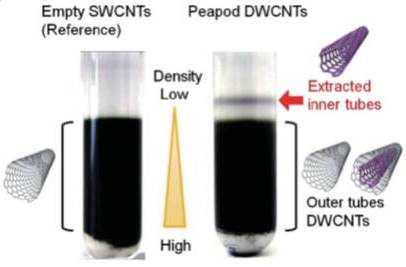 ジャーナル フリーCarbon nanotube possesses one-dimensional tubular structure whose diameter typically ranges from 0.4 to 5 nm. Recently, significant research efforts have been devoted to encapsulate various atoms and molecules into inner space of carbon nanotubes to create novel hybrid one-dimensional materials. In this paper, we review recent studies on carbon nanotubes encapsulating atoms and molecules, where the following topics are discussed in detail:formation of metal atomic wires in carbon nanotubes, structure and dynamics of the atomic wires, chirality control of carbon nanotubes based on fusion reaction in carbon nanotubes and extraction of materials from carbon nanotubes.抄録全体を表示PDF形式でダウンロード (1207K)
 -
板東 義雄, Chunyi ZHI, Dmitri GOLBERG原稿種別: 研究紹介
2012 年 33 巻 10 号 p. 569-574
発行日: 2012/10/10
公開日: 2012/10/27
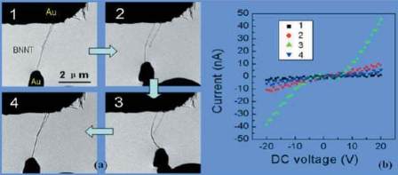 ジャーナル フリーThe hexagonal form of boron nitride (h-BN) is analogous to graphite with a layered structure. BN nanotube is one of the most important non-carbon nanotubes. Compared to the carbon nanotube, BN nanotube shows an electrically insulator, having a high chemical stability, excellent mechanical properties, and a high thermal conductivity. In this review, we report novel synthesis of BN nanotubes and nanosheets for high purity and high yield growth. We will also introduce in-situ TEM observations on mechanical and electrical properties measurements from individual BN nanotube and nanosheet. The polymeric composites containing BN nanotubes will be demonstrated for improvement of the insulating high thermal conductivity.抄録全体を表示PDF形式でダウンロード (1144K)
 -
嘉数 誠, 佐藤 寿志, Michal KUBOVIC原稿種別: 研究紹介
2012 年 33 巻 10 号 p. 575-582
発行日: 2012/10/10
公開日: 2012/10/27
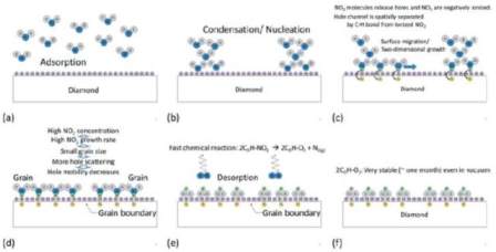 ジャーナル フリーThe hole channel of hydrogen (H)-terminated diamond surface can be linked to adsorption of a specific gas species on the surface. O3, NO2, NO, and SO2 were identified as adsorbates, which induce holes on the H-terminated diamond surface. During NO2 adsorption, hole sheet concentration, ps, saturated at a certain value, however, in the NO2 gas concentration range of>300 ppm, the values were the same. Therefore we determined that the high limit of ps is∼9×1013 cm−2, which is 5.7% of the surface C-H bonds for (001) orientation. X-ray photoelectron spectroscopy investigation showed upward band bending and partial oxidation but no C-N bonds of the H-terminated surface after exposure to air and NO2. We propose a NO2 adsorption/desorption and hole-doping model to explain these experimental results.抄録全体を表示PDF形式でダウンロード (958K)
 -
大曲 新矢, 吉武 剛原稿種別: 研究紹介
2012 年 33 巻 10 号 p. 583-588
発行日: 2012/10/10
公開日: 2012/10/27
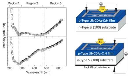 ジャーナル フリーUltrananocrystalline diamond/hydrogenated amorphous carbon composite (UNCD/a-C:H) film is a new candidate material applicable to optoelectronic devices owing to its unique electrical and optical properties. This paper describes a recent progress in the research on the application of semiconducting UNCD/a-C:H films to photodetectors. p-Type conduction accompanied by an enhancement in the carrier concentration was realized by boron doping. Spectral response measurement showed obvious photocurrent in the wavelength of shorter than 280 nm and above 500 nm, which probably originate from UNCD grains and mid-gap states owing to grain boundaries, respectively. Photodiodes comprising p-type UNCD/a-C:H films and n-type Si substrates exhibited a clear response for deep-ultraviolet light, and the external quantum efficiency and responsivity were more than 70% and 130 mA/W, respectively. It was experimentally proved that UNCD/a-C:H is a potential material for the application to photodetectors.抄録全体を表示PDF形式でダウンロード (1169K)
談話室
海外研究体験記
-
岩谷 克也2012 年 33 巻 10 号 p. 589-590
発行日: 2012/10/10
公開日: 2012/10/27
ジャーナル フリーPDF形式でダウンロード (394K)
先端追跡
-
2012 年 33 巻 10 号 p. 591
発行日: 2012/10/10
公開日: 2012/10/27
ジャーナル フリーPDF形式でダウンロード (167K)
- |<
- <
- 1
- >
- >|