- |<
- <
- 1
- >
- >|
-
久保 利隆2016 年37 巻8 号 p. 341
発行日: 2016/08/10
公開日: 2016/08/20
ジャーナル フリーPDF形式でダウンロード (165K)
-
藤井 慎太郎, 小本 祐貴, 多田 朋史, 大須賀 孝史, 村瀬 隆史, 藤田 誠, 木口 学原稿種別: 論文
2016 年37 巻8 号 p. 342-347
発行日: 2016/08/10
公開日: 2016/08/20
 ジャーナル フリー
We demonstrate tuning of charge transport properties through stacks of aromatic molecules on the single molecular scale. The stacks of aromatic molecules are formed in a molecular cage through a self-assemble process, in which non-covalently bound π-stacks act as replaceable modular components with adjustable electronic functions. Scanning tunneling microscopy-based break junction methods revealed that the insertion of the same pairs of aromatic molecules into the cage induces high electronic conductivity (10−3–10−2G0, G0 = 2e2/h), while different donor and acceptor pairs develop additional electronic diode properties. The rectification ratio was estimated to be 1.5–10. Theoretical calculations demonstrate that this rectification behavior originates from the distinct stacking order of the internal aromatic components against the electron-transport direction and the corresponding lowest unoccupied molecular orbital conduction channels localized on one side of the molecular junctions.
抄録全体を表示PDF形式でダウンロード (922K) -
井澤 哲美, 髙島 健悟, 山本 貴博原稿種別: 研究紹介
2016 年37 巻8 号 p. 348-353
発行日: 2016/08/10
公開日: 2016/08/20
 ジャーナル フリー
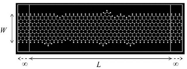
Effects of edge disorder on thermoelectric performance of graphene nanoribbons (GNRs) were investigated through computational simulations based on the non-equilibrium Green's function method combined with the tight-binding approximation. We found that the thermoelectric power factor PF can be optimized by adjusting the ribbon length, L, of GNRs with edge disorder concentration Cd. For example, at room temperature, PF of zigzag-edged GNRs at the Fermi energy shows a maximum value of 33 mW/(m K2) when Cd = 10% and L = 210 nm. Both the maximum PF and optimum L decrease with increasing Cd. The maximum PF is theoretically explained in terms of the crossover from the ballistic transport regime to the Anderson's localization regime.
抄録全体を表示PDF形式でダウンロード (679K) -
飯田 真一, Gregory L. FISHER, John S. HAMMOND, Scott R. BRYAN, 宮山 卓也原稿種別: 研究紹介
2016 年37 巻8 号 p. 354-358
発行日: 2016/08/10
公開日: 2016/08/20
 ジャーナル フリー
Recently, applications of TOF-SIMS have expanded into a wide variety of organic materials, because the sensitivity of high mass molecular ions was improved dramatically. However, it was very difficult to determine the chemical formula from the measured mass above m/z 200. The ambiguous peak identification was a significant problem in TOF-SIMS. In order to determine the chemical formula as well as detailed chemical structure, we developed the TOF-SIMS instrument equipped with MS/MS, and applied it to the various organic materials. In this article, we will introduce this unique instrument, and demonstrate the results of the spectra analyses by using MS/MS.
抄録全体を表示PDF形式でダウンロード (795K) -
—超硬工具基材への応用—奥村 洋史, 峰 和久原稿種別: 研究紹介
2016 年37 巻8 号 p. 359-362
発行日: 2016/08/10
公開日: 2016/08/20
 ジャーナル フリー
Auger electron spectroscopy (AES) was used to determine the concentration of W atoms diffused into a Co region across a WC/Co interface in a tungsten carbide tool. Direct analysis near the WC/Co interface by AES is difficult because of backscattering. We propose a practical method that considers backscattering in estimating the W concentration across the interface. We prepared a WC/Co model specimen with negligible diffusion of W into the Co region. We confirmed that the backscattering component in AES line profiles across the interface was reproduced by using a Monte Carlo (MC) code. Then, we measured AES line profiles over a WC/Co/WC region in a real tungsten carbide tool and calculated profiles without W diffusion into the Co region by the MC code. We estimated the W distribution in the Co region by considering backscattering, and subtracted the calculated profile from the measured profile to remove the backscattering component.
抄録全体を表示PDF形式でダウンロード (550K) -
一ノ倉 聖, 保原 麗, 高山 あかり, 長谷川 修司, Andrey V. MATETSKIY, Leonid V. BONDARENKO ...原稿種別: 研究紹介
2016 年37 巻8 号 p. 363-368
発行日: 2016/08/10
公開日: 2016/08/20
 ジャーナル フリー
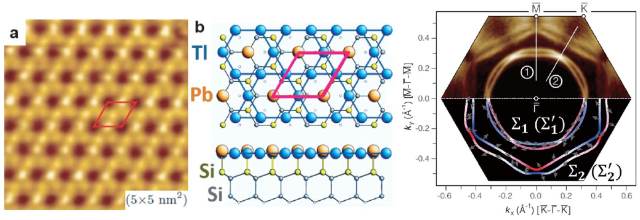
A surface reconstruction consisting of one monolayer of Tl and one-third monolayer of Pb on a Si(111) was found to exhibit a large Rashba-type spin splitting in the metallic surface-state bands together with two-dimensional superconductivity. Temperature dependent angle-resolved photoelectron spectroscopy revealed a strong electron-phonon interaction in one of the bands. In situ four-point-probe resistivity measurements with and without magnetic field demonstrated that the (Tl, Pb)/Si(111) system transited into the superconducting state at 2.3 K. The (Tl, Pb)/Si(111) is a prototypical system for prospective studies of intriguing properties of the space-inversion-symmetry-broken superconductor.
抄録全体を表示PDF形式でダウンロード (902K) -
奥田 直人, 平井 悠司, 下村 政嗣原稿種別: 研究紹介
2016 年37 巻8 号 p. 369-373
発行日: 2016/08/10
公開日: 2016/08/20
 ジャーナル フリー
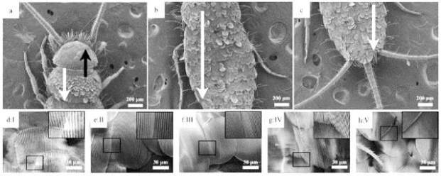
Friction is one of the great problems for wide variety of field, including insects, because of wearing of their body surfaces. Therefore, we focused on firebrat, because they live under bark and small cavity, and their surface would evolve for protection from wearing. In this report, surface observations by using field emission scanning electron microscope (FE-SEM) and friction measurements by using atomic force microscope (AFM) of firebrat body surfaces were carried out. As results, observations by using FE-SEM revealed that firebrats have many scales with groove structure, and groove period was non-uniformity around the head. Friction measurements by using AFM cleared that friction force was different from scanning direction and probe tip diameters. It is suggested that firebrat may reduce average friction forces and protect from wearing by using scales with non-uniformity groove structure.
抄録全体を表示PDF形式でダウンロード (1101K) -
—シリセン,ゲルマネンの創製を目指して—黒澤 昌志, 大田 晃生, 洗平 昌晃, 財満 鎭明原稿種別: 研究紹介
2016 年37 巻8 号 p. 374-379
発行日: 2016/08/10
公開日: 2016/08/20
 ジャーナル フリー
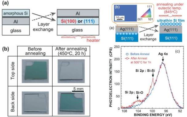
Two-dimensional (2D) honeycomb sheet of Si and Ge, known as silicene and germanene, respectively, is a promising material for next-generation group-IV electronics. Most researchers have synthesized them by deposition of Si or Ge atoms on metal substrates. On the other hand, this paper proposes a unique technique for synthesizing these 2D honeycomb sheets on Ag-covered Si or Ge substrate by using Ag-induced layer exchange (ALEX) process. Our method enables surface segregation of Si or Ge atoms from the underlying substrate by tuning annealing condition during ALEX. We believe that the present study is a first step towards creation of 2D honeycomb sheets on a Si chip.
抄録全体を表示PDF形式でダウンロード (962K) -
横山 喬大, Thang Duy DAO, Kai CHEN, 石井 智, Ramu Pasupathi SUGAVANESHWAR, 長尾 ...原稿種別: 研究紹介
2016 年37 巻8 号 p. 380-385
発行日: 2016/08/10
公開日: 2016/08/20
 ジャーナル フリー
We have developed narrow-band mid-infrared thermal emitters based on refractory plasmonic perfect absorbers operative at very high temperature. Colloidal mask etching was adopted to Mo-Al2O3-Mo trilayers to realize large-scale and cost-effective fabrication of periodically arrayed disk resonators. Using molybdenum and aluminum oxide as refractory components, high temperature operation was demonstrated up to 1000°C or even higher while retaining the excellent thermal stability and narrow-band emission comparable to that of noble metal plasmonic emitters. The narrow-band emission peaks can be tuned flexibly from 3 to 8 μm which overlaps well with the spectral region of molecular fingerprints. The proposed wavelength-selective thermal emitters can be used for various applications such as energy-saving high-power infrared heaters as well as for light sources for active infrared sensor systems.
抄録全体を表示PDF形式でダウンロード (1857K)
-
岡本 薫, 阿部 芳巳, 上田 茂典原稿種別: 論文
2016 年37 巻8 号 p. 386-391
発行日: 2016/08/10
公開日: 2016/08/20
 ジャーナル フリー
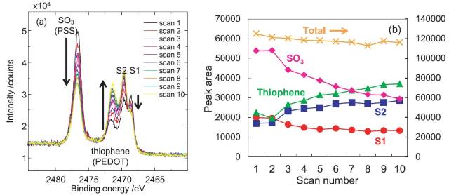
Metal/organic interfaces in organic thin-layer photovoltaic cells were investigated by means of hard X-ray photoelectron spectroscopy (HAXPES). The large detection depth of HAXPES using 6 keV X-rays allowed to study the buried organic layer, poly (3,4-ethylenedioxythiophene) : polystyrene sulfonate (PEDOT : PSS), through the Ag electrode. PEDOT : PSS showed two additional S 1s peaks at the Ag electrode interface, which could be associated with thiolate-like species and Ag sulfides. The latter peak increased after the high-humidity test, indicating that the interface reaction proceeded during the test. Severe X-ray-induced damage of PEDOT : PSS layer was also observed, mainly due to the transformation of sulfonate groups of PSS to the lower oxidation-state forms. Nevertheless, HAXPES showed to be one of the powerful tools to study the buried interface of organic devices as it is.
抄録全体を表示PDF形式でダウンロード (592K)
-
寺嶋 淳2016 年37 巻8 号 p. 392-393
発行日: 2016/08/10
公開日: 2016/08/20
 ジャーナル フリー
食中毒の原因は化学物質,自然毒から細菌やウイルスなどの病原体によるものまで多様であるが,本稿では細菌が原因となって発生する食中毒について述べる。細菌性食中毒の主要な原因菌も時代とともに推移しており,1990年代後半には,サルモネラと腸炎ビブリオが突出して多い傾向があったが,現在ではカンピロバクター菌による食中毒が多く,腸炎ビブリオ及びサルモネラによる食中毒は激減した。一方,近年の食材・食品流通の広域化にともなって,同一汚染源が疑われる広域の食中毒が発生することも最近の食中毒の特徴と言える。また,生肉や調理不十分な食肉の喫食が原因と考えられる食中毒が多いことから,食生活の変化も細菌性食中毒の発生状況と密接に関連しているものと考えられる。
抄録全体を表示PDF形式でダウンロード (365K)
-
菅 滋正2016 年37 巻8 号 p. 394-395
発行日: 2016/08/10
公開日: 2016/08/20
ジャーナル フリーPDF形式でダウンロード (337K)
-
2016 年37 巻8 号 p. 396
発行日: 2016/08/10
公開日: 2016/08/20
ジャーナル フリーPDF形式でダウンロード (1202K)
-
2016 年37 巻8 号 p. 397
発行日: 2016/08/10
公開日: 2016/08/20
ジャーナル フリーPDF形式でダウンロード (159K)
- |<
- <
- 1
- >
- >|